IC Packaging

Dedicated to Being Your Preferred Solution Provider Pushing the limits worldwide
Our Products
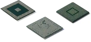
SPIL provides comprehensive packaging, offering lead frame base and substrate base packages, with either wire bond or flip chip interconnections. These packages satisfy most applications for customers serving the PC, hand-held product, consumer product and wire communication markets.
Besides the conventional SOP and QFP packages, SPIL has been devoted to the development of wafer thinning, fine-pitch wire bonding, stacked-die bonding, wafer bumping and flip-chip assembly technologies in order to realize advanced packages like: QFN, PBGA, TFBGA, Stacked-die CSP, WLCSP and FCBGA.
In order to meet our customer's future packaging requirements, we are continuously developing the next generation assembly technologies. Currently studies include: Through Silicon Vias, Integrated Passive Devices and 3D-SiP/3D-SIC packaging solutions.